Keeping Secrets in Hardware:
the Microsoft XBox
TM
Case
Study
Andrew "bunnie" Huang
AI Memo 2002-008
May 26, 2002
©
2
0
0
2
m
a
s
s
a
c
h
u
s
e
t
t
s
i
n
s
t
i
t
u
t
e
o
f
t
e
c
h
n
o
l
o
g
y,
c
a
m
b
r
i
d
g
e
,
m
a
0
2
1
3
9
u
s
a
--
w
w
w.
a
i
.
m
i
t
.
e
d
u
m
a
s
s
a
c
h
u
s
e
t
t
s
i
n
s
t
i
t
u
t
e
o
f
t
e
c
h
n
o
l
o
g
y
--
a
r
t
i
f
i
c
i
a
l
i
n
t
e
l
l
i
g
e
n
c
e
l
a
b
o
r
a
t
o
r
y
@ MIT
Abstract
This
paper
discusses
the
hardware
foundations
of
the
cryptosystem
employed
by
the
Xbox
TM
video
game
console
from
Microsoft.
A
secret
boot
block
over-
lay
is
buried
within
a
system
ASIC.
This
secret
boot
block
decrypts
and
verifies
portions
of
an
external
FLASH-type
ROM.
The
presence
of
the
secret
boot
block
is
camouflaged
by
a
decoy
boot
block
in
the
external
ROM.
The
code
contained
within
the
secret
boot
block
is
transferred
to
the
CPU
in
the
clear
over
a
set
of
high-speed
busses
where
it
can
be
extracted
using
simple
custom
hardware.
The
paper
concludes
with
recommendations
for
improving
the
Xbox
security
system.
One
lesson
of
this
study
is
that
the
use
of
a
high-performance
bus
alone
is
not
a
sufficient
security
measure,
given
the
advent
of
inexpensive,
fast
rapid
prototyping
services
and
high-performance
FPGAs.
2
1
Introduction
and
Background
Every
cryptosystem
is
based
on
some
kind
of
secret,
such
as
a
key.
Regardless
of
the
cipher,
the
security
of
a
cryptosystem
is
only
as
strong
as
the
secrecy
of
the
key.
Thus,
some
of
the
most
startlingly
effective
attacks
on
a
cryptosystem
involve
no
ciphertext
analysis,
but
instead
find
flaws
in
the
protocols
that
manage
the
keys.
Cryptosystems
based
on
symmetric
ciphers
are
particularly
vulnerable
to
protocol
attacks,
since
both
the
sender
and
the
receiver
must
be
trusted
to
have
a
copy
of
the
same
secret
key.
Despite
the
difficulty
of
key
management
in
symmetric
ciphers,
they
remain
attractive
because
of
their
algorithmic
simplicity
and
high
throughput
when
compared
to
public
key
ciphers.
Symmetric
cipher
key
management
becomes
especially
problematic
when
the
re-
ceiving
party
is
not
trusted
or
is
in
a
position
that
can
be
easily
compromised.
This
is
where
tamper-resistant
hardware
comes
into
play;
a
summary
of
tamper-resistance
guidelines
can
be
found
in
[6].
Many
systems
employ
tamper-resistant
hardware
tech-
niques
in
varying
degrees,
including
the
Sandia
National
Labs'
"Stronglink"
microme-
chanical
24-bit
lock
[2],
the
Clipper
chip
[1],
IBM's
4758
PCI
Cryptographic
Copro-
cessor
[3],
Cryptographic
Smartcards
[5]
[4],
Automatic
Teller
Machines
(ATMs),
and
now,
video
game
consoles.
However,
trusting
inadequate
physical
security
measures
to
protect
important
secrets
is
risky.
[14]
and
[15]
present
examples
of
how
some
of
the
aforementioned
tamper-resistant
systems
can
be
defeated
with
surprisingly
simple
and
direct
methods.
In
the
case
of
the
Xbox
TM
video
game
console
from
Microsoft,
the
secret
being
protected
is
a
key
and
an
algorithm
for
decrypting
and
verifying
a
bootloader.
This
bootloader
then
decrypts
and
verifies
a
kernel
image.
Both
the
bootloader
and
ker-
nel
image
are
contained
in
an
unsecured
FLASH
ROM.
The
kernel
then
verifies
the
authenticity
and
integrity
of
the
applications
it
runs.
Thus,
a
chain
of
trust
is
grown,
bottom
up,
from
a
seed
of
trust.
This
seedthe
secret
key
and
an
algorithmis
planted
in
a
physically
secure,
secret
boot
block.
The
Xbox
architecture
results
in
the
deployment
of
large
number
of
identical
de-
vices,
all
of
which
contain
the
same
secret
information.
As
the
analysis
below
illus-
trates,
the
security
of
such
a
system
can
be
readily
compromised,
even
if
the
secret
is
protected
by
tamper-resistant
hardware
and
obscured
by
algorithmic
complexity.
2
Xbox
Hardware
Cryptosystem
Overview
The
Xbox
crypto
protocol
presents
a
strong
defense
in
the
face
of
unsecured
FLASH
ROM-based
modifications.
Please
refer
to
figure
1.
The
Xbox
boots
from
a
512-byte
secret
boot
block
that
is
hard-coded
into
the
southbridge
system
ASIC
(the
"MCPX").
This
boot
block
performs
the
following
functions,
in
order:
Ż
loads
the
"jam
tables",
i.e.,
initializes
the
console
chipset
Ż
turns
on
the
processor
caches
Ż
decrypts
the
kernel
bootloader,
contained
in
FLASH
ROM
Ż
verifies
that
decryption
was
successful
Ż
jumps
to
the
decrypted
kernel
bootloader
3
The
bootloader
then
performs
some
more
system
initialization,
decrypts
a
kernel
image
from
FLASH
ROM,
decompresses
and
verifies
the
decrypted
image,
and
enters
the
kernel.
The
kernel
decryption
key
is
stored
within
the
bootloader
image.
Note
that
the
secret
boot
block
code
is
structured
so
that
the
bootloader
decryption
key
is
never
written
to
main
memory,
thus
defeating
an
attack
that
involves
eavesdropping
on
the
main
memory
bus.
The
bootloader
is
encrypted
with
RC-4
using
a
128-bit
key.
The
decryption
algo-
rithm
and
key
are
stored
in
the
secret
boot
block
and
executed
by
the
Pentium
CPU;
the
busses
between
the
secret
boot
block
and
the
CPU
are
not
encrypted
but
assumed
to
be
secure
due
to
their
high
speeds.
The
decryption
of
the
bootloader
image
is
veri-
fied
by
checking
for
a
32-bit
magic
number
near
the
end
of
the
plaintext
stream.
This
check
only
ensures
that
the
ciphertext
stream
was
not
corrupted;
one
with
knowledge
of
the
secret
key
and
the
magic
number
can
easily
create
original
bootloader
images.
It
is
fairly
clear
from
the
code
structure
of
the
secret
boot
block
that
such
a
simple,
unreliable
check
was
employed
because
there
was
not
enough
space
for
anything
else.
The
magic
number
check
might
also
confuse
efforts
to
create
original
bootloader
code
based
on
a
key
obtained
without
full
knowledge
of
the
secret
boot
block's
contents,
such
as
through
a
personnel
leak
or
brute
force.
However,
a
brute
force
approach
to
re-
covering
the
bootloader
is
probably
out
of
the
question,
since
distributed.net's
"bovine"
effort,
running
for
over
4
years
and
currently
capable
of
testing
over
100
gigakeys/s,
is
still
working
on
a
64-bit
RC-5
cipher
at
the
time
of
writing
[7].
Given
this
secure
boot
protocol,
modifying
the
contents
of
the
FLASH
ROM
alone
will
stand
a
very
low
chance
of
revealing
anything
useful
about
the
console
1
.
This
is
compounded
by
the
fact
that
the
FLASH
ROM
contains
a
decoy
boot
block
with
halfway
reasonable
looking
decryption
and
initialization
code.
The
algorithm
in
the
decoy
boot
block
is
a
bastardized
RC-4,
and
of
course
applying
this
algorithm
on
the
ROM
contents
yields
nothing
but
white
noise.
Further
discussion
on
how
the
secret
boot
block
was
discovered
is
contained
in
the
next
section.
3
Breaking
the
Physical
Security
This
section
provides
a
chronology
of
how
the
Xbox's
physical
security
was
reverse
engineered.
Reading
out
the
FLASH
ROM
contents
and
tracing
the
processor's
execution
start-
ing
from
the
boot
vector
proved
to
be
futile,
as
the
contents
of
the
boot
block
in
the
FLASH
ROM
were
a
decoy,
cleverly
designed
to
thwart
such
activity.
The
code
within
the
FLASH
ROM
boot
block
followed
the
same
general
flow
as
the
code
within
the
secret
boot
block,
but
the
decryption
algorithm,
the
keys
and
the
ciphertext
start
loca-
tion
were
incorrect.
This
initially
resulted
in
a
great
deal
of
confusion
but
was
later
explained
by
the
discovery
of
the
secret
boot
block
overlay.
The
realization
of
the
existence
of
a
secret
boot
block
happened
as
a
result
of
the
observation
that
overwriting
the
processor
reset
vector
in
the
FLASH
ROM
has
no
effect
on
the
Xbox
boot
sequence.
This
led
to
a
series
of
experiments
that
mapped
out
1
An
important
exception
recently
discovered
is
described
in
section
6.
4
controllers
key-locked
hard disk
(executeables,
cached data,
save games)
pentium
CPU
NV2A
northbridge
+ gfx
MCPX
southbridge
SDRAM
64 MB
FLASH
ROM
(bootloader
+ OS kernel)
secret boot
ROM
DVD drive
(game data /
executeables)
game
controllers
dongles w/
executeables
(DVD player,
etc.)
IDE
HyperT
SSTL-2
GTL+
64/
32+
128/
21+
8/
2
legacy
8/
24+
133
MHz
200
MHz
DDR
200
MHz
DDR
< 10
MHz
secure hardware boundary
security relationship
not yet known
trusted code
and data:
digitally signed
with Microsoft
private key
bus width:
data/others
bus clock
rate
100Base-T
USB
Figure
1:
Overview
of
the
Microsoft
Xbox
hardware.
5
the
extent
of
the
secret
boot
block.
The
block
is
believed
to
be
512
bytes
in
length,
situated
at
the
highest
location
in
processor
physical
memory.
The
following
approaches
were
then
considered
for
extracting
the
secret
boot
block
contents:
Ż
decapping
the
MCPX
southbridge
ASIC
Ż
using
the
JTAG
boundary
scan
on
the
Pentium
to
step
through
the
"real"
boot
se-
quence
Ż
probing
the
main
memory
bus
for
any
portions
of
the
boot
block
that
were
written
to
memory
Ż
probing
the
processor-northbridge
bus
using
a
logic
analyzer
or
custom
hardware
Ż
probing
the
HyperTransport
northbridge-southbridge
bus
using
custom
hardware
The
direct
approach
of
decapping
the
MCPX
southbridge
ASIC
was
rejected
be-
cause
this
ASIC
appears
to
be
manufactured
in
a
0.13
process
with
perhaps
6
or
7
metal
layers
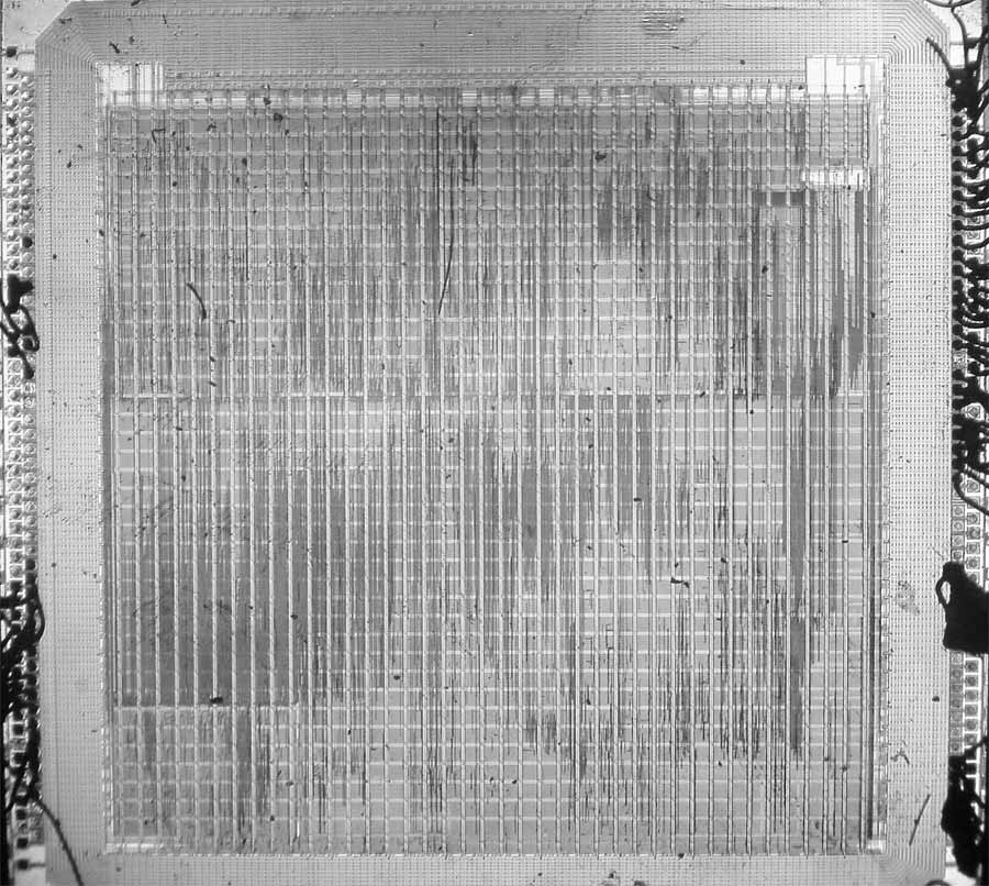
(figure
2).
Extracting
the
bootblock
from
this
ASIC
would
require
a
de-
layering
facility
and
access
to
an
electron
microscope.
While
there
are
companies
such
as
Chipworks
that
specialize
in
these
kinds
of
services,
it
is
a
difficult,
expensive,
and
time-consuming
task.
Figure
2:
Die
shot
of
the
MCPX
Southbridge
ASIC
The
JTAG
boundary
scan
approach
was
rejected
on
the
grounds
that
the
TRST#
pin,
used
to
hold
the
JTAG
chain
in
reset,
was
tied
active
in
a
manner
that
was
difficult
to
modify
without
removing
the
processor.
Removal
and
socketing
of
the
processor
was
considered
to
be
prohibitively
expensive
and
time
consuming;
the
cost
of
a
BGA
socket
for
the
Pentium
III
is
estimated
to
be
in
the
hundreds
to
thousands
of
dollars.
In
addition,
the
JTAG
boundary
scan
codes
for
the
Pentium
III
are
largely
proprietary
and
would
have
to
be
reverse
engineered
as
well.
SDRAM
probing
was
rejected
on
the
grounds
that
far
too
many
pins
(128
data
pins
6
alone)
had
to
be
simultaneously
probed,
and
on
the
grounds
that
the
decryption
routine
and/or
key
could
be
held
entirely
in
processor
cache
and
never
written
to
SDRAM.
Also,
the
cost
of
solder-on
TQFP-100-to-logic-analyzer
adapters
is
prohibitive
(around
$600
per
adapter;
four
are
required).
Probing
the
processor-northbridge
bus
was
re-
jected
for
similar
reasons:
at
least
64
data
pins
had
to
be
probed,
and
tapping
such
a
large
number
of
GTL+
signals
without
causing
signal
integrity
issues
was
thought
to
be
very
difficult.
The
northbridge-southbridge
bus,
however,
showed
promise
because
of
its
sim-
plicity.
The
bus
has
a
low
signal
count
(10
unique)
and
all
the
signal
traces
are
laid
out
on
the
console's
motherboard
in
a
straight
flow-through
fashion
(12-mil
center-to-
center
spacing
within
a
differential
pair,
13-mil
spacing
between
differential
pairs,
see
figure
4).
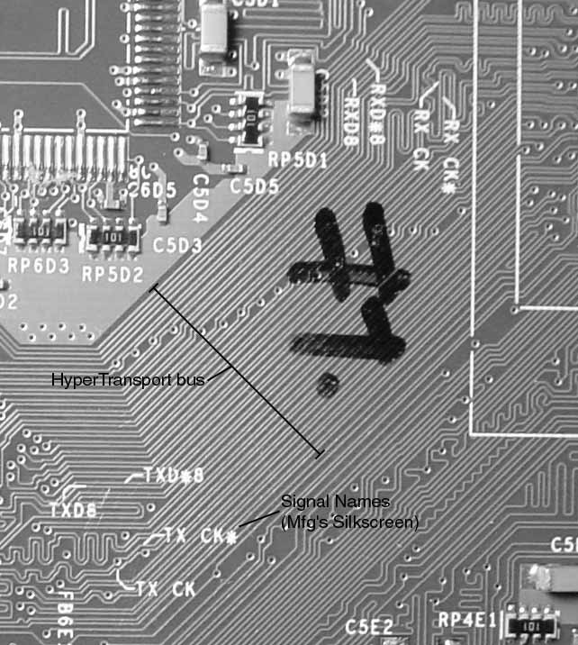
In
addition,
the
clock
and
strobe
signals
for
both
the
transmit
and
receive
directions
are
clearly
labeled
on
the
motherboard,
perhaps
for
manufacturing
debug
and
test
reasons
(figure
3).
Data
on
the
nVidia
nForce
chipset
[9],
a
close
relative
to
the
Xbox
chipset,
indicates
that
the
bus
uses
the
HyperTransport
(formerly
known
as
Lightning
Data
Transport
(LDT))
protocol.
The
specifications
for
the
HyperTransport
protocol
are
open
and
readily
available.
[8]
Figure
3:
HyperTransport
bus
layout
showing
silkscreen
information
The
primary
difficulties
in
tapping
the
HyperTransport
bus
are
its
high
speed
(200
MHz
DDR)
and
its
use
of
differential
signaling
(few
logic
analyzers
come
with
support
for
differential
signaling).
It
is
interesting
to
note
that
HyperTransport
bus
protocol
7
analyzers
are
commercially
available
from
vendors
such
as
FuturePlus,
but
they
cost
upward
of
$25,000.
This
price
does
not
include
the
high-end
logic
analyzer
required
to
drive
the
protocol
analyzer.
The
alternative
solution
to
tapping
the
northbridge-southbridge
HyperTransport
bus
was
to
build
a
relatively
cheap,
fully
custom,
differential-to-single-ended
"Tap
Board",
and
to
connect
the
output
of
this
board
to
an
FPGA.
A
Xilinx
Virtex-E
part
was
used
in
this
study
because
it
was
readily
available,
as
it
was
used
as
part
of
the
author's
thesis
work;
however,
a
better
choice
would
be
any
of
the
new
Xilinx
Virtex-II
FPGAs.
A
suitable
Virtex-II
FPGA
would
cost
about
$50
in
single
quantities.
The
custom
Tap
Board
uses
a
two-layer,
6
mil
trace/space,
15
mil
hole
process
from
Advanced
Circuits,
offered
at
a
price
of
$33
per
board
in
small
quantities.
A
Texas
Instruments
SN65LVDS386
LVDS-to-TTL
converter
was
used
to
turn
the
differential
HyperTransport
signals
into
a
single-ended
format.
It
turns
out
that
the
HyperTransport
physical
signaling
specification
is
similar
to
LVDS,
but
with
a
different
common-mode
offset.
The
output
of
the
converter
drives
a
cable
to
the
FPGA
board.
The
FPGA
is
configured
to
receive
the
high
speed
signals
with
the
CTT
(Center-Tap
Terminated)
"Select
I/O"
option.
CTT
is
chosen
because
it
allows
the
single-ended
TTL
drivers
to
be
terminated
with
a
low
impedance
to
1.5V
and
still
function
properly.
Note
that
although
Virtex-E
FPGAs
support
LVDS
directly,
the
target
FPGA
board
was
not
originally
designed
to
support
the
LVDS
configuration.
12 mil
13 mil
12 mil
differential signal pair
6 mil
trace
Figure
4:
Dimensions
of
the
HyperTransport
signal
traces
on
the
motherboard.
The
Tap
Board
has
on
one
edge
a
pattern
of
traces
with
no
soldermask
that
matches
the
pattern
of
traces
on
the
Xbox
motherboard.
The
Tap
Board
was
soldered
directly
to
the
Xbox's
northbridge-southbridge
bus.
Only
the
receive-direction
Tap
Board
was
mounted
for
this
study.
The
mating
edge
was
shaped
using
a
belt
sander,
so
that
the
tapping
traces
were
flush
with
the
edge
of
the
board,
and
the
board
could
be
mounted
at
a
reclined
angle
to
enhance
solderability.
The
soldermask
on
the
Xbox
was
removed
with
fine-grit
sand
paper,
and
the
Tap
Board
was
carefully
aligned
by
hand,
and
then
held
roughly
in
place
by
soldering
a
coarse
piece
of
wire
between
the
Tap
Board
and
the
motherboard.
A
hard-setting
adhesive,
such
as
Miller-Stephenson
Epoxy
907,
was
ap-
plied
to
fix
the
angle
and
mating
distance
of
the
Tap
board
to
the
motherboard;
once
the
epoxy
was
cured,
the
holding
wire
was
removed,
and
the
traces
between
the
Tap
Board
8
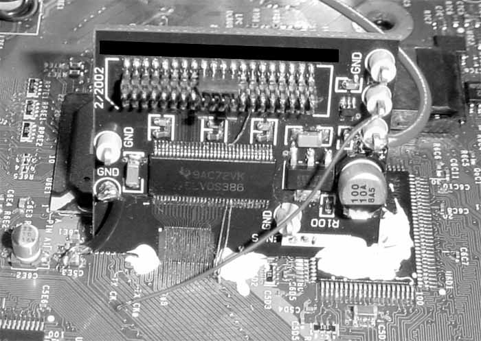
and
the
Xbox
motherboard
were
easily
soldered
using
a
fine-tip
iron
and
a
microscope.
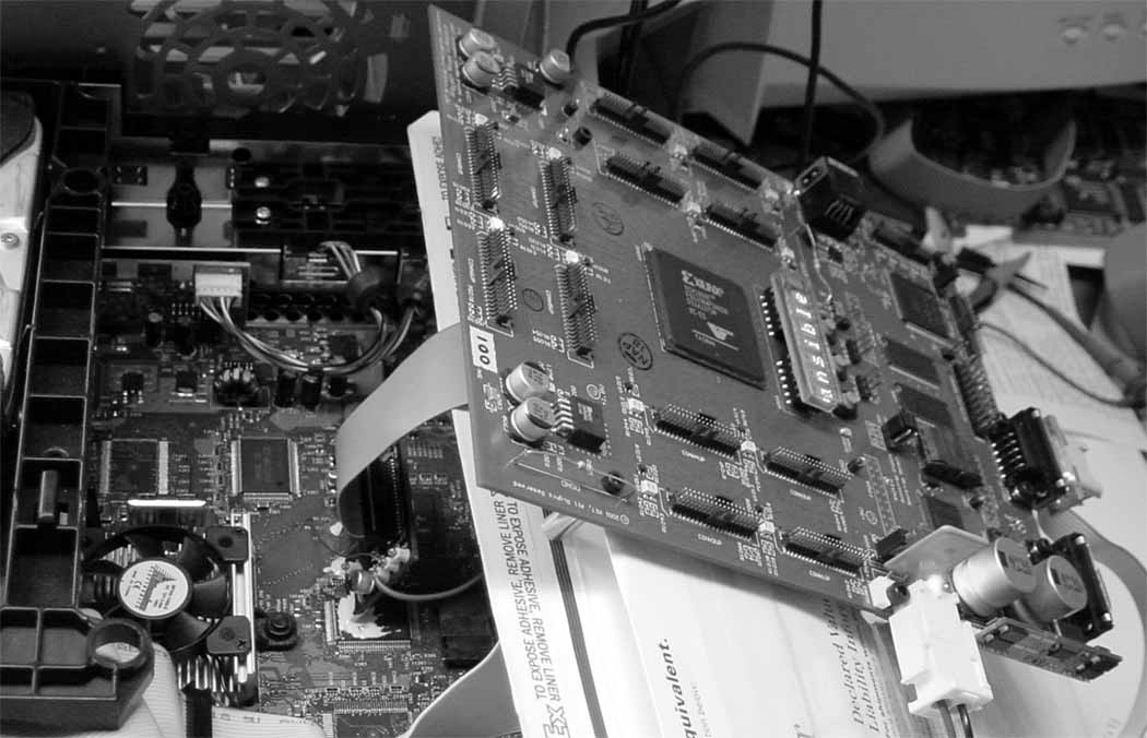
Figure
5:
Tap
Board
connected
to
the
FPGA
board.
The
FPGA
board
was
originally
developed
by
the
author
for
another
work.
The
polarity
of
the
HyperTransport
bus
signals
was
determined
by
probing
the
idle
state
of
the
wires,
assuming
that
their
idle
state
had
a
value
of
0x00.
Those
signals
that
had
the
positive
and
negative
pairs
swapped
relative
to
the
Tap
board
layout
idled
to
a
"1".
Signals
with
inverted
polarity
were
restored
to
their
true
value
within
the
trace
capture
FPGA.
Figure
6:
Close-up
of
the
Tap
Board
mounted
in
the
Xbox
A
Xilinx
Virtex-E
FPGA
was
used
to
capture
traces
of
HyperTransport
bus
activ-
ity.
It
was
difficult
getting
the
FPGA
to
manage
the
200
MHz
DDR
data
rates
with
9
low
skew.
However,
careful
hand-layout
of
the
input
registers,
post-layout
timing
sim-
ulations
at
nominal
temperature
and
voltage,
and
iterations
to
manually
tweak
delays
and
skews
eventually
centered
the
clock
signal
within
the
data
signal
on
the
FPGA's
input
registers.
The
retimed
data
was
then
demultiplexed
to
a
very
manageable
100
MHz
single-data
rate
32-bit
wide
bus
and
written
into
a
bank
of
FIFOs,
along
with
a
sequence
count
that
recorded
at
what
cycle
relative
to
a
reset
signal
the
data
was
captured.
Some
additional
logic
was
incorporated
into
the
FPGA
that
discarded
idle
values
(0x0000
0000)
from
the
trace
FIFOs
and
formatted
the
deserialized
data
relative
to
the
strobe
signal,
clearly
identified
on
the
Xbox
motherboard
as
"RXD8
/
RXD*8"
(figure
3)
in
sector
5D
(the
Xbox
motherboard
has
a
coordinate
system
printed
on
its
periphery).
The
reset
signal
can
be
determined
by
probing
traces
near
the
HyperTransport
bus
that
behaved
like
a
reset
signal.
In
reality,
it
is
possible
that
some
signal
that
was
not
the
true
reset
signal
was
used
to
trigger
the
trace
capture,
but
that
is
irrelevant
as
the
signal
chosen
seemed
to
display
a
consistent
timing
relationship
with
respect
to
the
bus.
In
fact,
the
signal
used
to
trigger
the
trace
capture
exhibited
a
350
ns
runt
pulse
about
67
ms
after
power-on-reset;
this
runt
pulse
was
filtered
out
by
a
state
machine,
as
it
was
erroneously
restarting
the
trace
capture.
Once
traces
of
data
were
captured
by
the
FPGA,
the
order
of
the
bits
on
the
Hy-
perTransport
bus
relative
to
the
Tap
Board
layout
could
be
determined.
This
can
be
done
by
correlating
known
values
in
the
FLASH
ROM
with
data
values
captured
on
the
HyperTransport
bus.
A
1's
count
can
be
used
to
identify
candidate
patterns
and
data
sequences
for
manual
correlation.
Fortunately,
very
early
on
in
the
trace
several
distinctive,
sequential
values
are
grabbed
from
the
FLASH
ROM:
a
few
values
from
the
lowest
address
in
FLASH
ROM,
followed
by
a
few
values
from
the
boot
vector,
which
happens
to
be
identical
between
the
decoy
FLASH
ROM
contents
and
the
secret
boot
ROM
contents.
The
order
of
the
traces
for
the
receive-direction
bus
on
the
moth-
erboard
are
believed
to
be,
from
the
outside
to
the
inside,
bit
8
(CTL
strobe),
4#,
0#,
7#,
2#,
3#,
CLK#,
5,
6#,
and
1#.
Signals
with
#
after
them
are
inverted
with
respect
to
the
Tap
Board
layout.
The
raw
trace
data
captured
by
the
FPGA
was
then
dumped
to
files
and
manually
processed.
An
example
illustrating
the
format
of
trace
data
can
be
found
in
figure
7.
The
sequence
number
was
critical
in
determining
the
boundaries
of
cache
traces;
blocks
of
8
or
16
words
are
fetched
by
the
processor,
even
when
the
caches
are
off.
Trace
data
was
differentiated
between
secret
boot
code
and
FLASH
ROM
data
by
searching
for
the
first
word
of
the
candidate
trace
in
a
dump
of
the
FLASH
ROM;
if
the
data
could
not
be
found
in
the
FLASH
ROM,
it
was
guessed
to
be
secret
boot
code.
Because
the
processor
boots
with
its
caches
off,
the
first
roughly
24
million
bus
cycles
contained
repeated
line
fills
of
the
"jam
table"
initialization
code,
and
were
ignored
as
they
just
performed
the
wrote
initialization
of
the
chipsets.
The
caches
were
then
turned
on
by
the
boot
code,
and
very
clear
and
simple
to
read
blocks
of
instructions
and
data
were
found.
These
instruction
traces
were
mapped
into
the
secret
boot
block
using
the
decoy
FLASH
ROM
boot
block
as
a
template.
The
recovered
block
of
code
was
then
disassembled,
and
the
decryption
algorithm
was
determined
to
be
128-bit
RC-4.
Because
the
location
of
the
128-bit
key
within
the
secret
boot
block
was
ambiguous
(the
Tap
Board
only
provides
data
traces
without
addresses),
a
brute-force
search
was
10
00000097
:
664A1D55
:::
E
:
000000C6
00000D5C
:
05F108F6
:::
F
:
01000000
00000DE0
:
2A1A2841
:::
1
:
CC003000
00000E5D
:
B6FE7F68
:::
E
:
A0552C01
00000EDA
:
5932C662
:::
1
:
000000FD
00000F57
:
F9FBA4C1
:::
E
:
C7C94000
00000FD4
:
F7F9B6AE
:::
1
:
000000C6
00001051
:
73376133
:::
E
:
9EC49400
000010CE
:
FD0127AD
:::
1
:
000000D6
0000114B
:
34E8FD29
:::
E
:
C7C94000
00001245
:
1814A022
:::
1
:
000000C6
000012C2
:
38EBD672
:::
E
:
C7C94000
00022526
:
C6C0847E
:::
1
:
000000C6
00022527
:
A26216BB
:::
E
:
C7C94000
00022528
:
99DA5F80
:::
E
:
000000C6
00022529
:
453862E3
:::
1
:
C7C94000
000226D5
:
B6DF18C0
:::
E
:
000000C6
000226D6
:
DA562768
:::
1
:
C7C94000
000226D7
:
0F1D66E3
:::
E
:
000000C6
000226D8
:
DDC59B59
:::
1
:
8D42CBCD
Figure
7:
An
example
illustrating
the
format
of
trace
data
captured
by
the
FPGA.
Format
of
the
data
is
"sequence
:
data
:::
aligner
:
unaligned
data".
utilized
to
help
isolate
the
key.
A
16-byte
sliding
"guess
key"
window
over
the
captured
data
trace
was
used
as
input
to
an
RC-4
decryption
engine,
and
a
histogram
of
the
data
output
was
used
to
determine
when
the
key
was
found.
This
information
helped
resolve
some
ambiguities
in
the
placement
of
the
data
within
the
secret
boot
block,
and
a
full
picture
of
the
important
code
within
the
secret
boot
block
was
assembled.
Now
that
the
secret
boot
procedure
is
understood,
it
is
possible
to
encrypt
a
new
ROM
for
the
Xbox
console,
and
to
further
study
the
structure
of
the
Xbox
bootloader
and
kernel.
Given
the
RC-4
algorithm,
the
128-bit
key,
and
the
magic
check
number
at
the
end
of
the
decrypted
segment,
one
can
run
original
code
on
the
Xbox.
4
Lessons
Learned
One
lesson
of
this
study
is
that
the
use
of
a
high-performance
bus
alone
is
not
a
suf-
ficient
security
measure;
the
advent
of
cheap,
fast
rapid
prototyping
services
and
high
performance
FPGAs
allows
even
poor
students
to
create
devices
that
can
tap
the
bus.
However,
encrypting
a
bus
introduces
its
own
problems.
A
secure
cipher
on
a
high
per-
formance
bus
significantly
impacts
latency,
power
consumption,
and
reliability.
Power
consumption
is
increased
because
the
activity
factor
for
the
bus
approaches
100%,
if
the
encryption
scheme
is
any
good.
In
this
case,
the
power
consumed
driving
the
bus
11
would
increase
by
over
an
order
of
magnitude,
as
the
observed
activity
factor
on
the
northbridge-southbridge
bus
was
well
below
10%.
Reliability
is
hurt
because
a
single
bit
error,
even
during
an
idle
cycle,
can
corrupt
large
blocks
of
data;
with
a
stream
cipher,
the
corruption
would
extend
until
the
stream
is
resynchronized.
A
compromise
solution
to
the
problem
is
to
simply
not
trust
any
bus
in
the
system.
In
this
case,
the
secret
boot
block
might
employ
a
digital
signature
protocol,
such
as
Authenticode
R
,
using
public
key
algorithms
and
one-way
hashes.
[10]
Then,
all
secu-
rity
rests
in
the
secrecy
of
the
private
key,
and
the
strength
of
the
public
key
algorithm.
In
order
to
prevent
employee
leaks
from
spreading
a
private
key,
a
system
similar
to
the
BBN
SignAssure
TM
could
be
used
to
manage
the
key
so
that
no
human
ever
has
knowl-
edge
of
the
private
key.
The
principal
drawback
of
this
method
is
that
it
requires
extra
silicon
area
to
be
spent
on
storing
a
larger
secret
boot
block,
as
it
is
probably
difficult,
if
not
impossible,
to
code
a
full
public
key
encryption
algorithm
plus
key
storage
and
hardware
initialization
code
within
512
bytes.
The
above
suggestion
does
not
prevent
someone
from
eavesdropping
and
obtaining
the
plaintext
of
the
operating
system
code,
but
it
does
effectively
defeat
any
attempt
to
run
original
code.
The
public
key
scheme
could
be
defeated,
however,
by
a
mech-
anism
that
snoops
the
main
memory
bus
and
patches
plaintext
in
main
memory.
As
discussed
previously,
this
approach
is
possible,
but
difficult;
however,
the
tenacity
of
an
attacker
should
not
be
underestimated.
For
example,
a
known
attack
on
the
Sony
Playstation2
console
was
developed
that
is
rumored
to
work
by
dynamically
patching
its
high-performance
RAMBUS
memory
system.
The
difficulty
of
a
memory
patch
at-
tack
could
be
increased
by
using
a
simple
periodic
hash
and
check
of
the
critical
code
regions
in
memory.
Buffer
overrun
exploits
are
also
a
point
of
weakness,
and
they
work
regardless
of
the
secret
boot
protocol.
An
attacker
sniffing
an
insecure
bus
could
obtain
the
de-
crypted
kernel
code
and
analyze
it
for
weaknesses.
However,
any
machine
architecture
that
employs
guarded
pointers
[11]
is
much
more
difficult,
if
not
impossible,
to
attack
using
buffer
overruns.
A
fast,
efficient
guarded
pointer
scheme
with
a
simple
hardware
implementation
is
described
in
[12].
This
scheme
can
easily
be
adapted
to
work
in
a
64-bit
architecture.
A.
Kerckhoffs
(1835-1903)
once
stated
that
the
security
of
a
cryptosystem
must
not
depend
on
keeping
the
algorithm
secret;
this
is
referred
to
as
Kerckhoffs'
Principle.
[13]
Another
way
of
stating
this
is
that
there
is
no
security
through
obscurity.
In
particular,
it
is
an
error
to
assume
that
a
secret,
distributed
along
with
the
information
it
guards,
is
never
revealed.
For
example,
the
Sega
Dreamcast
uses
a
proprietary
GD-ROM
software
format;
but,
the
drive
can
read
CD-ROM
disks.
The
discovery
of
a
back
door
in
the
Dreamcast
OS
allowed
executables
to
be
run
directly
from
a
standard
CD-ROM,
thus
nullifying
the
barrier
presented
by
the
proprietary
GD-ROM
format.
Other
systems
that
rely
on
well-hidden
secrets,
including
the
Clipper
chip
[14]
and
the
smartcards
used
widely
throughout
Europe
to
control
access
to
services
such
as
pay-TV,
cell
phones
and
gas,
have
been
shown
to
be
surprisingly
vulnerable.
[15]
In
this
case,
the
Tap
Board
and
trace
capture
FPGA
design
was
developed
in
spare
time
over
the
duration
of
three
weeksincluding
the
5-day
turn
time
for
board
fabricationfor
a
total
cost
of
around
$50
per
board.
In
other
words,
if
you
ship
your
secrets
in
your
hardware,
it
is
a
good
assumption
that
the
users
will
eventuallyand
perhaps
quicklyknow
your
secrets.
12
The
failure
of
the
Microsoft
Xbox
console
security
protocol
is
compounded
by
the
fact
that,
as
a
console
manufacturer,
design-for-test
and
design-for-manufacturability
is
paramount.
Creating
a
console
with
too
much
security
makes
it
difficult
to
debug
and
manufacture.
For
example,
the
backside
of
the
Xbox
motherboard
is
populated
with
test
pointsincluding
test
points
for
every
pin
on
the
FLASH
ROM.
These
were
originally
installed
because
of
the
desire
to
quickly
test
for
faults
during
manufactur-
ing.
The
flip
side
is
that
one
could
build
a
custom
"bed-of-nails"
tester
jig
that
uses
the
the
FLASH-ROM
test
points
to
reprogram
Xbox
motherboards
with
any
desired
code.
This
method
would
be
fast,
inexpensive
and
solder-free.
The
lesson
here
is
that
even
if
a
manufacturer
is
very
confident
about
their
trust
model
and
security
protocols,
it
must
guard
against
the
possibility
that
they
may
someday
be
broken.
To
this
extent,
a
sim-
ple
physical
security
measure,
such
as
a
spray-on
conformal
coating,
would
severely
hamper
the
re-use
of
test
structures
for
improper
purposes.
This
of
course
greatly
com-
plicates
the
repair
of
hardware
failures
in
the
field,
but
that
is
a
business
trade-off
the
manufacturer
must
make.
A
more
radical
alternative
would
be
to
design
the
gaming
system
using
proprietary
hardware
and
proprietary
media
formats,
thus
limiting
the
practical
impact
of
any
at-
tack
on
the
console.
Game
consoles
are
manufactured
in
very
high
volumes,
so
the
cost
of
developing
a
simple
but
effective
proprietary
format
can
be
amortized.
The
format
could
then
be
patented,
providing
protection
against
unauthorized
use
without
the
need
for
secrecy.
This
approach
was
taken
by
Nintendo
with
their
Nintendo
64
console.
[16]
Although
patents
have
a
20
year
lifetime,
this
is
an
eternity
in
the
video
game
console
industry:
the
original
Nintendo
Entertainment
System
(NES)
had
its
debut
in
1985.
5
Future
Work
Understanding
the
secret
Xbox
boot
protocol
is
just
the
first
step
in
understanding
the
Xbox.
It
is
now
possible
to
investigate
the
kernel
and
bootloader
in
more
detail.
It
has
been
determined
that
the
kernel
is
also
encrypted
with
RC-4/128,
and
it
is
also
believed
to
be
compressed
using
LZX
compression,
a
scheme
employed
by
Microsoft's
canonical
distribution
format,
the
"Cabinet"
file.
The
structure
and
function
of
the
kernel
is
still
being
investigated.
One
important
issue
to
investigate
is
the
privacy
of
users
who
use
the
Xbox
for
on-
line
tasks.
It
is
known,
through
a
parallel
effort
of
the
author,
that
information
such
as
the
serial
number
of
the
console
is
stored
electronically
and
is
probably
accessible
to
the
kernel.
What
happens
to
this
information
when
the
Xbox
is
plugged
into
the
internet?
Because
of
the
encryption
used
to
secure
the
Xbox,
the
nature
of
the
information
that
is
relayed
to
Microsoft's
on-line
game
servers
is
unknown.
Thus,
important
future
work
is
to
try
to
determine
what
the
Xbox
reveals
about
the
user's
identity
and
personal
gaming
habits.
13
6
Addendum
It
has
recently
been
called
to
the
author's
attention
that
the
hardware
initialization
pro-
cedure
of
the
Xbox
contains
a
significant
weakness.
[17]
Recall
from
section
2
that
the
first
step
in
the
Xbox
boot
process
is
to
load
the
"jam
tables"
that
configure
the
console's
chipsets.
This
jam
table
initialization
procedure
involves
a
lengthy
and
com-
plex
sequence
of
writes
to
various
memory-mapped
hardware
register
locations.
As
a
result,
the
initialization
procedure
is
implemented
using
a
simple
bytecode
interpreter
that
reads
initialization
commands
and
data
from
the
FLASH
ROM.
These
bytecode
commandsstored
as
plaintextcan
be
manipulated
to
cause
the
initialization
procedure
to
abort
before
the
kernel
decryption/verification
routine
is
executed,
and
to
instead
run
insecure
code
directly
out
of
the
FLASH
ROM.
In
other
words,
with
plaintext-only
modifications
in
the
FLASH
ROM,
one
can
entirely
bypass
the
Xbox's
security
mech-
anism.
One
could
easily
fix
this
security
hole,
however,
by
verifying
the
jam
table's
contents
prior
to
bytecode
execution
with
a
one-way
hash
function,
or
by
explicitly
coding
all
initialization
functions
within
the
secure
boot
block.
Both
of
these
solutions,
however,
would
require
the
secure
boot
block
to
grow
significantly
from
its
current
512-byte
size,
and
neither
solution
allows
easy
changes
to
the
initialization
procedure
in
case
a
bug
is
found
or
in
case
the
hardware
evolves
as
a
result
of
cost
reduction
efforts.
Acknowledgments
The
author
would
like
to
acknowledge
the
support
of
the
on-line
electronic
community.
The
author
would
also
like
to
thank
the
Electronic
Frontier
Foundation
for
providing
legal
counsel.
Hal
Abelson
and
Tom
Knight
also
provided
invaluable
moral
support.
Finally,
the
author
would
like
to
thank
Nikki
Justis
for
all
her
love
and
support,
and
for
giving
him
such
an
interesting
toy
for
Christmas.
References
[1]
Federal
Information
Processing
Standards
Publication,
FIPS
PUB
185:
Escrowed
Encryption
Standard
(EES)
http://www.itl.nist.gov/fipspubs/fip185.htm
[2]
Thomas
W.
Krygowski,
Jeffry
J.
Sniegowski,
M.
Steven
Rodgers,
Stephen
Montague,
James
J.
Allen,
Jerome
F.
Jakubczak,
Samuel
L.
Miller,
Infras-
tructure,
Technology
and
Applications
Of
Micro-Electro-Mechanical
Systems
(MEMS),
Sandia
National
Laboratories,
Intelligent
Micromachine
Department,
http://www.mdl.sandia.gov/Micromachine,
also
appears
in
Sensor
Expo
1999.
[3]
IBM,
IBM
4758
PCI
Cryptographic
Coprocessor,
http://www.ibm.com/security/cryptocards/
[4]
Gemplus
(a
smartcard
vendor),
Gemplus
Corporate
Website,
http://www.gemplus.com
14
[5]
Pil
Joon
Lee,
Eun
Jeong
Lee,
Yong
Duk
Kim,
How
to
Implement
Cost-Effective
and
Secure
Public
Key
Cryptosystems
Proceedings
of
the
First
International
Work-
shop
on
Cryptographic
Hardware
and
Embedded
Systems
(CHES),
August
1999.
[6]
Federal
Information
Processing
Standards
Publication,
FIPS
PUB
140-2:
Security
Requirements
for
Cryptographic
Modules,
http://csrc.nist.gov/publications/fips/fips140-2/fips1402.pdf
[7]
distributed.net,
distributed.net:
Project
RC5,
http://www.distributed.net/rc5/
[8]
HyperTransport
Consortium,
HyperTransport
TM
I/O
Link
Specification,
Version
1.03,
http://www.hypertransport.org
[9]
nVidia
Corporation,
nForce
MCP
Product
Overview,
06.01v1,
http://www.nvidia.com
[10]
Microsoft
Developer
Network,
Introduction
to
Code
Signing,
http://msdn.microsoft.com/workshop/security/authcode/intro
authenticode.asp
[11]
Nicholas
P.
Carter,
Stephen
W.
Keckler,
and
William
J.
Dally,
Hardware
support
for
fast
capability-based
addressing,
Proceedings
of
ASPLOS
VI,
October
1994,
pp.
319-27.
[12]
Jeremy
Brown,
J.P.
Grossman,
Andrew
Huang,
and
Thomas
F.
Knight,
Jr.,
A
capability
representation
with
embedded
address
and
nearly-exact
object
bounds,
Project
Aries
Technical
Memo
5,
http://www.ai.mit.edu/projects/aries/Documents/Memos/ARIES-05.pdf
[13]
Auguste
Kerckhoffs,
La
cryptographie
militaire,
Journal
des
sciences
militaires,
vol.
IX,
pp.
5-38,
Jan.
1883,
pp.
161-191,
Feb.
1883.
[14]
R.
Anderson
and
M.
Kuhn,
Tamper
Resistance
-
a
Cautionary
Note,
Proceedings
of
the
Second
Usenix
Workshop
on
Electronic
Commerce,
pp.
111,
November
1996.
[15]
R.
Anderson
and
M.
Kuhn,
Low
Cost
Attacks
on
Tamper
Resistant
Devices,
IWSP:
International
Workshop
on
Security
Protocols,
LNCS,
1997.
[16]
Van
Hook,
et
al.,
High
Performance
Low
Cost
Video
Game
System
with
Co-
processor
Providing
High
Speed
Efficient
3D
Graphics
and
Digital
Audio
Signal
Processing,
U.S.
Patent
6,239,810,
May
29,
2001.
[17]
Private
conversation
with
visor.
visor
can
be
reached
by
sending
a
personal
mes-
sage
to
visor
on
www.xboxhacker.net
15